Linee di ricerca
The Department of Physics aims to promote thematic projects, including those of an interdisciplinary nature, both within the University (coordinating in its activity with other Departments) and through external actions with national research organizations.
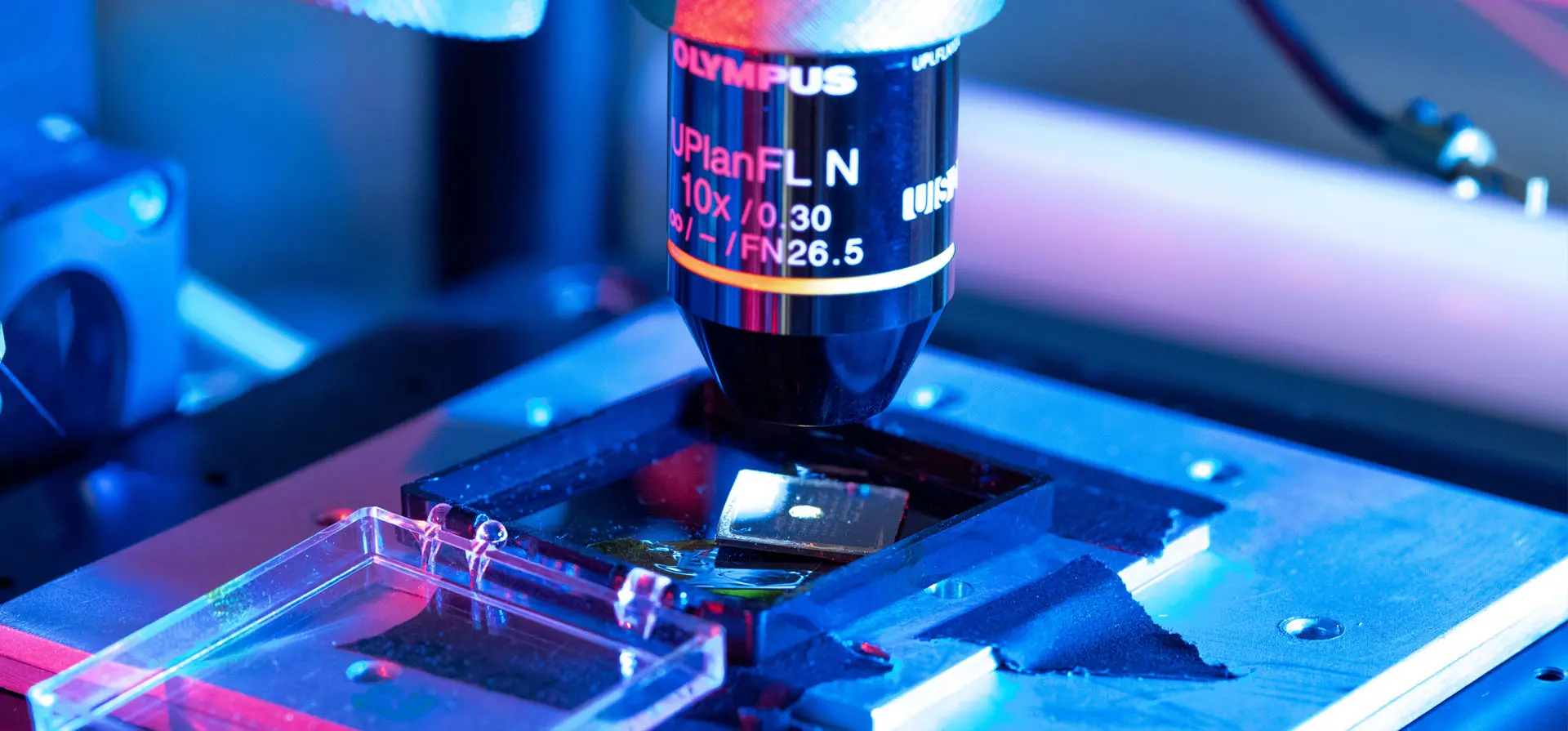
Ultrashort light pulse generation and applications to the study of ultrafast phenomena in the matter
The research activity concerns the development of new laser sources for the generation of ultrashort optical pulses (in the femtosecond regime) and their application to the study of dynamical processes in materials. This research exploits state-of-the-art technologies and methodologies in the field of lasers, with important implications in non-linear optics, optical communications and material diagnostics. The main research projects are:
- Generation of few-optical-cycle laser pulses for extreme non-linear optics applications (generation of high-order harmonics;
- Attosecond pulses and related technologies;
- Application of femtosecond pulses to the study of electronic state dynamics in low-dimensional materials, such as nanoparticles, polymers and in general carbon-based nano-structured materials;
- Ultrashort laser sources tunable from the near-infrared to the visible-ultraviolet, for spectroscopical applications with high temporal resolution;
- Scanning Near-Field Optical Microscopes (SNOM) with high spatial and temporal resolution for nano-optical applications. These research projects are part of the research activities of the ULTRAS research centers and the IFN at the Department of Physics.
The above projects are also part of the research activity of the Istituto di Fotonica e Nanotecnologie (IFN) of the Consiglio Nazionale delle Ricerche (CNR) The realized instrumentation is part of the "Centre for Ultrafast Science and Biomedical Otics" (CUSBO) European Facility, considered by the EU as an "European Large Scale Infrastructure" for its innovative characteristics.
Solid state lasers and photonic devices for integrated systems
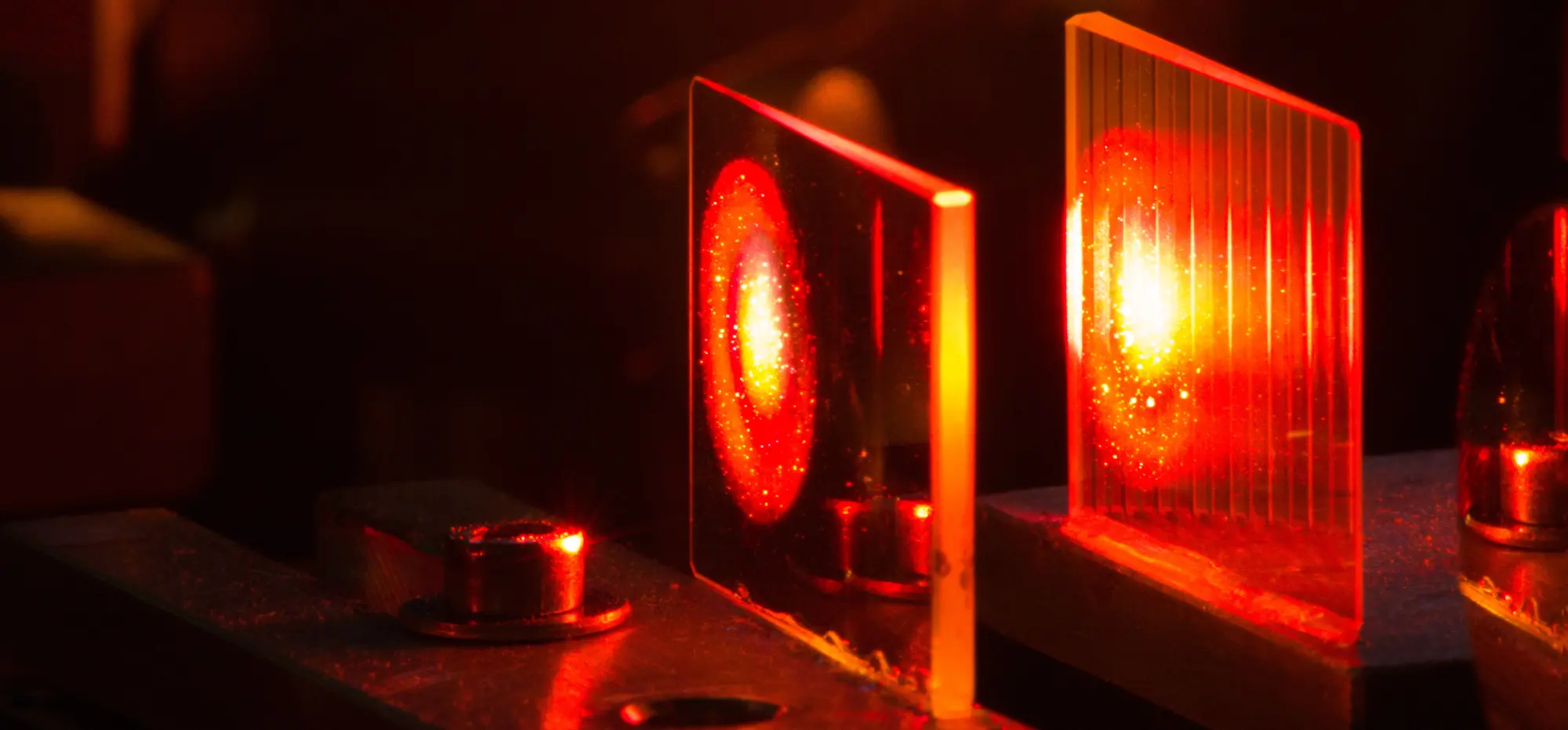
The research activity concerns the development of solid state lasers and integrated photonic devices for application to environmental monitoring, telecommunications and coherent control of light. This research is characterized by a highly innovative content. In particular, on one hand it aims at a deep comprehension of the basic physical phenomena underlying the topics of interest, on the other hand it intends to find new and forefront solutions in the addressed application fields. The main research projects are:
Active integrated optical devices for the realization of waveguide amplifiers and lasers operating in the third telecommunications window;
Frequency-stabilized solid state lasers, based on innovative active materials, for metrology and environmental monitoring;
Micro-fabrication, by means of femtosecond laser pulses, of photonic devices for telecommunications and microfluidic;
Fiber optic lasers and amplifiers for telecommunications and environmental monitoring;
Guided waves nonlinear optics for all-optical devices and solitonic propagation;
Fiber gratings and periodic optical structures for coherent control of light.
The above projects are also part of the research activity of the Istituto di Fotonica e Nanotecnologie (IFN ↗ (http://www.ifn.cnr.it/)) of the Consiglio Nazionale delle Ricerche (CNR ↗ (http://www.cnr.it/)).
Photonics for health, food and cultural heritage
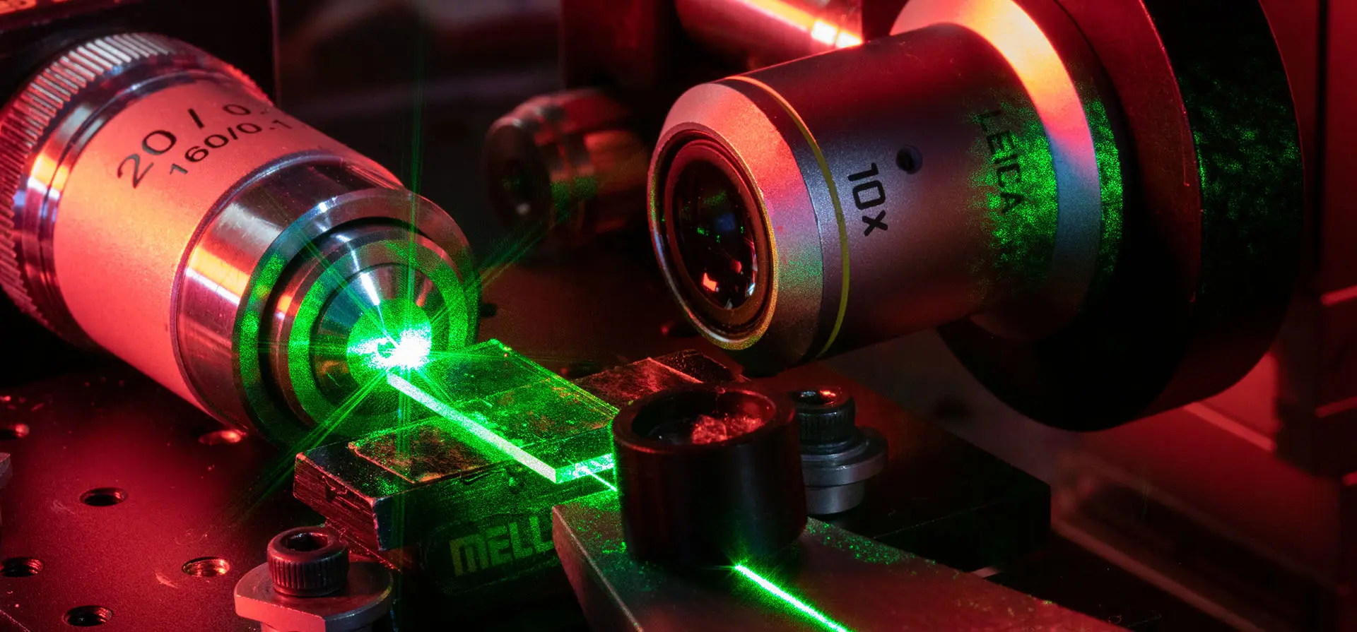
The research takes place at the Physics Department of the Politecnico di Milano through a network of 14 cutting-edge laboratories dedicated to the development of new methods and innovative techniques based on photonics and mainly aimed at non-invasive diagnostic applications in several areas, including biomedical, agri-food and cultural heritage. The common feature of all methods of investigation is the development of novel instruments aimed at the measurement of light with high temporal resolution and sensitivity. The main diagnostic principles are related to the analysis of fluorescence emission and propagation of optical radiation in highly diffusive media. The applicative vocation of this research line has led to the successful implementation of both laboratory instrumentation and portable devices in compliance with national and international regulations. These results have enabled the transfer of the technological innovation to hospital, clinical and museum environments.
The research line is also part of the activities of the Institute of Photonics and Nanotechnology (IFN ↗ (http://www.ifn.cnr.it/)) and the National Research Council (CNR ↗ (http://www.cnr.it/)). The laboratories and their instrumentation are part of the facility "Centre for Ultrafast Science and Biomedical Optics" (CUSBO ↗ (http://www.cusbo.polimi.it/)) of Laserlab Europe, accredited as "European Large Scale Infrastructure" by the European Union.
Epitaxial growth and nanostructure fabrication
Magnetic nanostructures
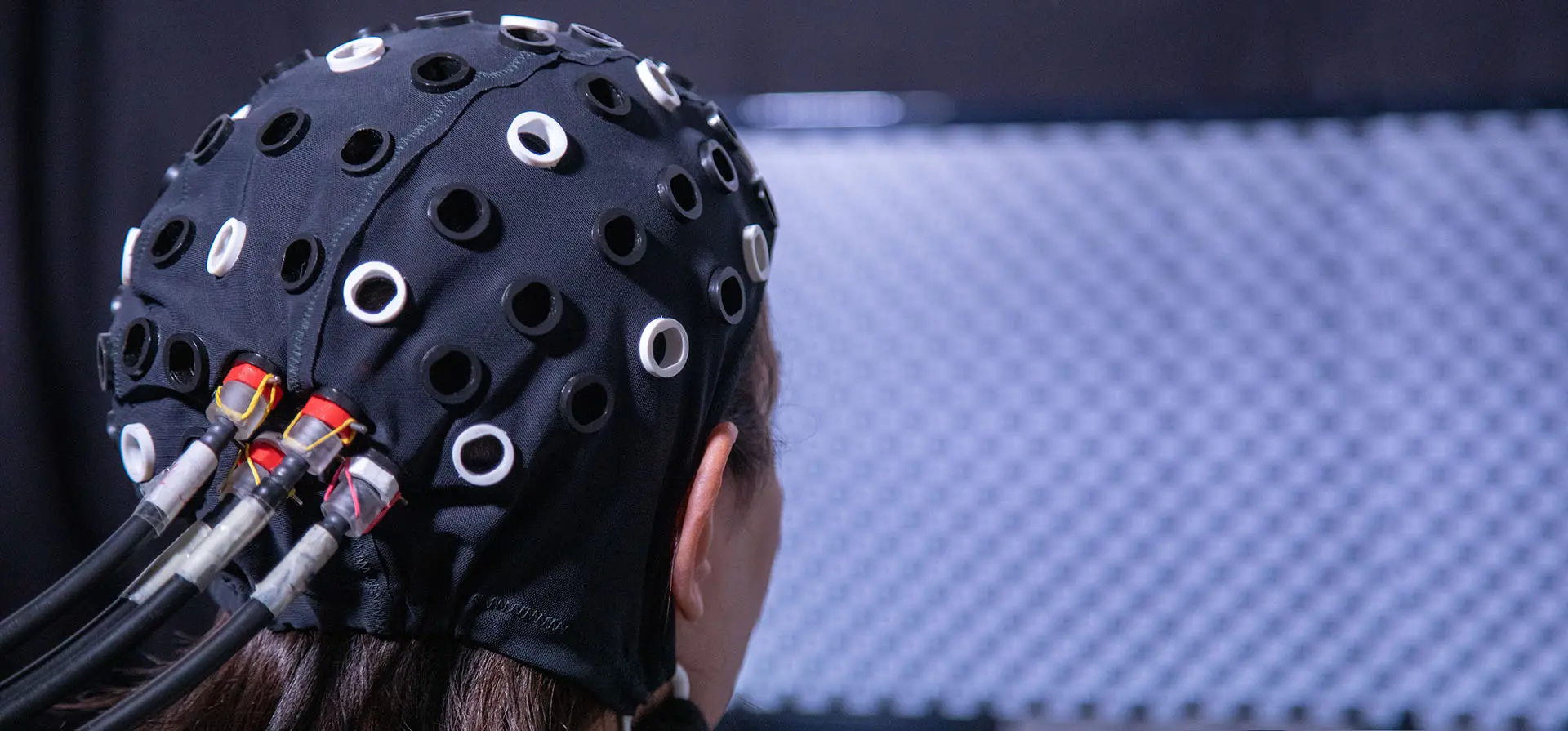
The activity is focused on the growth of nanostructured artificial materials (typically layers of nano- or subnanometric thickness) and on their characterization by means of several spectroscopy and microscopy techniques.
In particular, magnetic materials spatially confined down to nanometric scales are investigated. Typical examples are given by ultrathin films with antiferromagnetic coupling, oxides thin films, ferromagnet/semiconductor interfaces, rare earths multilayers and transition metals multilayers.
These innovative structures are synthesized by vacuum deposition on single crystal substrates, using either Pulsed Laser Deposition (PLD) or Molecular Beam Epitaxy (MBE).
The samples are characterized in-situ by means of diagnostic tools such as diffraction of low/high energy electrons (LEED and RHEED, respectively), Auger spectroscopy (AES), x-ray and ultraviolet photoemission spectroscopy (XPS and UPS), photoelectron diffraction (XPD). The electronic and magnetic properties are investigated in-situ by means of electron spectroscopies - also with spin resolution - and techniques based on the magneto-optical Kerr effect (MOKE). The latter technique is also performed with spatial resolution (ex-situ) and variable temperature (down to 10 K), for the investigation of statistical fluctuations in the process of magnetic hysteresis.
A further activity devoted to the lateral definition of nanostructures by means of lithographic techniques (both with light and electron beams), together with an ion beam etching system (IBE), has been recently started. Deposition by sputtering is also available for the realization of electrical contacts and for the growth of different materials, insulators too. Transport and magneto-transport properties are investigated by performing measurements taking advantage of a helium cryostat with a superconducting magnet.
Dealing with micro- and nano-structures, it is certainly important to have access to microscopy techniques. In such a field, the activities deal both with well-estabilished optical microscopies (confocal microscopy) and scanning probe techniques, such as Scanning Near-field Optical Microscopy (SNOM), Scanning Tunneling, Atomic and Magnetic Force Microscopy (STM, AFM and MFM), and finally with chemical sensitive electron microscopy (SAM, Scanning Auger Microscopy).
All the research lines are integrated within the activities of the Center of Excellence for NanoEngineered Materials and Surfaces (NEMAS(link is external)), instituted by the Italian Ministry for University and Research (MIUR(link is external)) at Politecnico di Milano, and of the Interuniversity Center (Politecnico di Milano and Università di Milano Bicocca) LNESS(link is external) (Laboratory of Epitaxial Nanostructures on Silicon and for Spintronics).
Semiconductor nanostructures
The laboratory for heterostructures and nanostructures on silicon, located at the centre LNESS(link is external) in Como, focuses on the fabrication and characterization of semiconductor thin films for microelectronic and optoelectronic applications. The laboratory has a substantial infrastructure, consisting of complementary state to the art deposition and analysis techniques. It is also equipped with clean-room facilities for photolithography, wet chemical processing, electron beam lithography and reactive ion etching.
One of the main strengths of the laboratory is undoubtedly the variety of epitaxial deposition techniques, ranging from molecular beam epitaxy (MBE) for compound semiconductors and oxides, ultra-high vacuum magnetron sputter epitaxy of group IV semiconductors to plasma assisted chemical vapour deposition.
Of particular relevance is low-energy plasma-enhanced chemical vapour deposition (LEPECVD). This process is ideally suited for the production of virtual substrates, consisting of relaxed SiGe alloy buffer layers on Si. These artificial substrates are used as platforms for subsequent epitaxy steps, with numerous applications in micro- and optoelectronics and photonics. Thus the laboratory is active in the fabrication of high-mobility SiGe/Si heterostructures, specializing on strained-Ge quantum wells with record low-temperature mobilities, photodetectors and modulators based on SiGe, and SiGe waveguides.Another area of major interest to the laboratory is monolithic integration of III-V semiconductors on Si substrates for applications in optoelectronics and especially high-efficiency solar cells.
Here, the laboratory’s expertise on oxide epitaxy by MBE provides a means for an alternative virtual substrate concept distinct from the aforementioned SiGe buffers. With the epitaxial oxide activity we also explore alternative concepts for gate oxides and novel devices based on thin oxide/Si combinations.
The laboratory also has a strong activity in nanodevices, where device fabrication is accomplished by combining electron beam lithography with optical lithography and reactive ion etching. The same techniques are used for substrate patterning for precise positioning of semiconductor nanostructures during self-assembled epitaxial growth.
The work on epitaxial hetero- and nanostructures is complemented by research on nanocrystalline silicon and its applications in low-cost photovoltaic cells and sensors.
Nanostructures at the liquid/solid interface
The lab research activity (Solid-Liquid Interface Nanomicroscopy and Spectroscopy - SoLINano-Sigma) is focused on the liquid/solid physics and on processes occurring on the electrode surface. These processes can produce adsorbate, ions and molecules super-structures, starting from solutes present in the used electrolyte. The lab offers the possibility of studying processes in real conditions and not in special vacuum environments. In particular, special super-structures can be obtained via electrochemical protocols that are exploited also in industrial processes. Recently, for example, new strategies for the electrode protection inside the batteries have been developed. The nanostructure characterization is obtained by using special microscopies, such as the electrochemical atomic force (EC-AFM) and scanning tunneling microscopy (EC-STM). A new spectroscopic system (Raman) will be coupled in the lab for a fully chemical surface characterization at the liquid/solid interface.
Electronic, optical and magnetic properties of low-dimensional systems
This activity is devoted to the fundamental electronic and magnetic properties of solids studied with electron spectroscopy and to the development of new experimental methods in that field.
The work is based on the design, the construction and the use of original and advanced instrumentation, capable of opening new paths in the field of spectroscopies based on ultraviolet radiation, x rays, or electron beams (see the list of instruments). For this reason in many cases our instruments can work only when coupled to the most modern electromagnetic radiation sources (synchrotrons, ultra-short pulse lasers). The instruments, usually designed and built in our Department, are installed and used in synchrotron radiation labs (AXES and IRRS at the ESRF, France; SAXES at the SLS in Switzerland) or at the ULTRAS lab of the INFM/CNR inside the Department (UphOS). The VESI lab (photoemission and inverse photoemission of samples grown in situ by MBE) and the SAM lab (scanning electron microscopy with Auger spectroscopy capability) are installed inside the Department’s building. In some cases the research activity is based also on instrumentation developed by other groups at the synchrotrons.
The current research projects are devoted to the characterization, at an atomic level, of the magnetic and electronic structure of materials potentially interesting for future applications of electronic technologies, such as magnetic oxides and superconductors. These materials stimulate also a purely scientific interest due to their very special properties that greatly challenge the best theoretical models. For example the project “High resolution RIXS” is devoted to high critical temperature cuprate superconductors, ferromagnetic manganite thin films, titanium and vanadium oxides; for those systems we aim at determining the relation between the local crystalline structure (coordination, interatomic distances) and the electronic energy levels. The “Hard RIXS” project is devoted to electronic excitations in strongly correlated systems too, with the possibility of studying the effects of pressure on electronic correlation. The “FemtoMagnetism and x-ray scattering” projects is based on the use of magnetic circular dichroism in special experimental geometries for the study, at atomic scale, of the magnetic dynamics in ferromagnets. The “Ultrafast electronic Dynamics in Solids” project is devoted to the study of electronic and magnetic dynamics.
