B3YOND
Website's ProjectB3YOND
Website's Project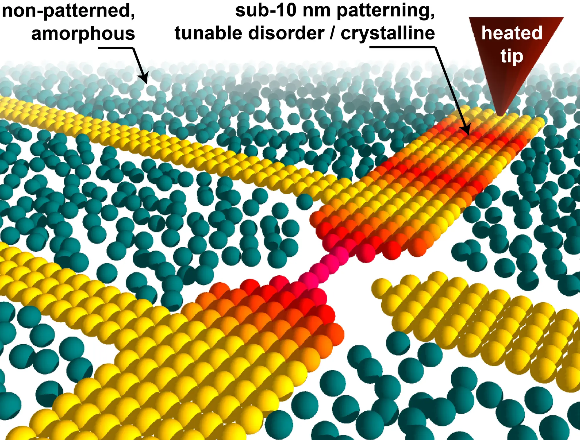
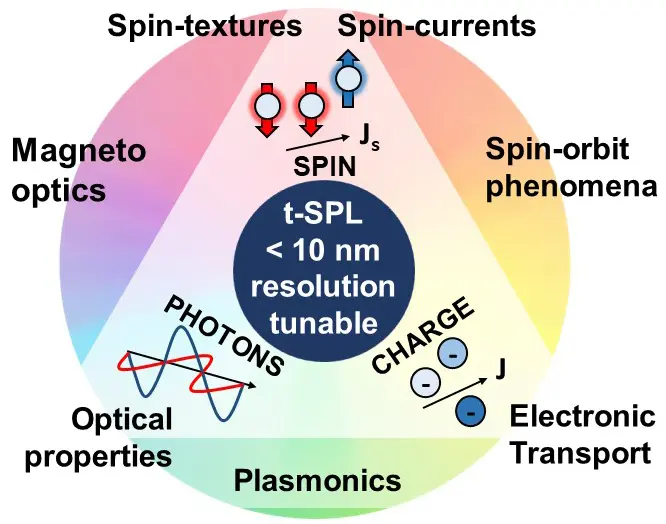
Nanoscale materials often exhibit intriguing and exotic properties not present in the same bulk materials. The explosion of nanomaterial characterisation techniques has significantly enhanced our understanding. In addition, the parallel development of nanofabrication techniques has enabled the practical realisation of numerous nanostructures and nanotechnologies. However, nanofabrication is facing physical limitations that pose a barrier to the continued downsizing of devices and practical applications that require exquisite control of nanoscale patterns and finely tuned physical properties. The EU-funded B3YOND project is developing a game-changing nanofabrication technique based on thermally assisted scanning probe lithography, and plans to use it to deliver novel artificial nanomaterials for 3D nanoelectronics and spintronics, ushering in a new era of nanotechnologies.
Publications
- D. Petti, S. Tacchi, and E. Albisetti, “Review on magnonics with engineered spin textures”, Journal of Physics D: Applied Physics 55, 293003 (2022). https://doi.org/10.1088/1361-6463/ac6465
- E. Albisetti, A. Calò, A. Zanut, X. Zheng, G.M. de Peppo, and E. Riedo*, “Thermal scanning probe lithography”, Nature Reviews Methods Primers 2, 32 (2022). https://doi.org/10.1038/s43586-022-00110-0
- S. Tacchi, J. Flores-Farías, D. Petti, F. Brevis, A. Cattoni, G. Scaramuzzi, D. Girardi, D. Cortés-Ortuño, R. A. Gallardo, E. Albisetti, G. Carlotti, P. Landeros, “Experimental observation of flat bands in one-dimensional chiral magnonic crystals”, Nano Letters 23, 14, 6776–6783 (2023); https://doi.org/10.1021/acs.nanolett.2c04215
- A. Barman, G. Gubbiotti, S. Ladak, A. O. Adeyeye, M. Krawczyk, J. Gräfe, C. Adelmann, Sorin Cotofana, A. Naeemi, V. I Vasyuchka, B.Hillebrands, SA Nikitov, H. Yu, D. Grundler, A. Sadovnikov, A.A. Grachev, S.E. Sheshukova, J.-Y. Duquesne, M. Marangolo, G. Csaba, W. Porod, V.E. Demidov, S. Urazhdin, S. Demokritov, E. Albisetti, D. Petti, et al., “The 2021 Magnonics Roadmap”, Journal of Physics: Condensed Matter (2021). https://doi.org/10.1088/1361-648X/abec1a
- V. Levati, D. Girardi, N. Pellizzi, M. Panzeri, M. Vitali, D.Petti, E. Albisetti, “Phase Nanoengineering via Thermal Scanning Probe Lithography and Direct Laser Writing”, Advanced Materials Technologies 8, 2300166 (2023); https://doi.org/10.1002/admt.202300166
- D. Girardi, S. Finizio, C. Donnelly, G. Rubini, S. Mayr, V. Levati, S. Cuccurullo, F. Maspero, J. Raabe, D. Petti, E. Albisetti, “Three-dimensional spin-wave dynamics, localization and interference in a synthetic antiferromagnet”, Nature Communications 15 (1), 3057 (2024); https://doi.org/10.1038/s41467-024-47339-9
- A. Del Giacco, F. Maspero, V. Levati, M. Vitali, E. Albisetti, D. Petti, L. Brambilla, V. Polewczyk, G. Vinai, G. Panaccione, R. Silvani, M. Madami, S. Tacchi, R. Dreyer, S. R. Lake, G. Woltersdorf, G. Schmidt, R. Bertacco, “Patterning Magnonic Structures via Laser Induced Crystallization of Yittrium Iron Garnet”, Advanced Functional Materials, 2401129 (2024); https://doi.org/10.1002/adfm.202401129