Harnessing photoexcited hot carriers – electrons and holes with energy far from equilibrium – is a long-standing goal in nanophotonics, promising breakthroughs to develop highly efficient photovoltaic devices, drive and control single molecule photochemistry, or to achieve ultrafast all-optical switching with metasurfaces. However, despite their enormous potential, realizing tailored nanostructures for real-world applications based on hot carriers remains an open challenge. One major roadblock lies in the inability to directly investigate hot carriers at their intrinsic space (Angstrom, 10-10 meters), time (femtoseconds, 10-15 seconds) and energy (electron volts) scales, due to the difficulty in attaining all the three resolutions simultaneously.
In a study recently published in Nature Communications, researchers from Politecnico di Milano and the Max Planck Institute for Solid State Research (MPI-FKF) have overcome this barrier by combining advanced modelling and femtosecond nonlinear spectroscopy. The team successfully captured the ultrafast dynamics of hot carriers at the atomic scale, offering an unprecedented window into their behaviour.
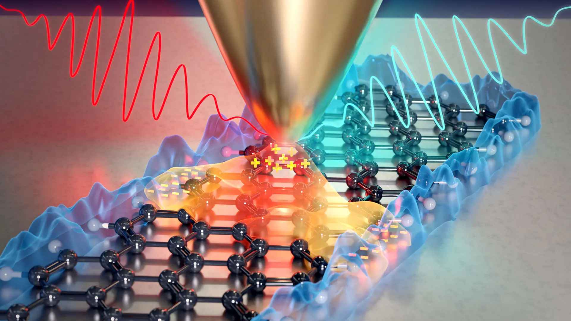
Using atomic scale femtosecond microscopy, they visualized hot electrons photoexcited in a gold picocavity – an optical cavity confied to sub-nanometer dimensions. The experiments revealed that hot carriers can be used to modulate a broadband anti-Stokes electronic resonance Raman scattering signal at ultrafast rates (up to tens of THz), with a recovery time under 150 femtoseconds - faster than typical carrier relaxation processes. This ability to optically control signals on such rapid timescales opens the door to novel all-optical switching schemes at atomic dimensions. Complementing the experiments, theoretical simulations shed light on the energy-dependent spatiotemporal evolution of the electronic dynamics, identifying key mechanisms driving the observed response.
The researchers further demonstrated the power of this technique by mapping the hot-carrier distribution and nonlinear optical responses in a single graphene nanoribbon. This atomic-scale nonlinear optical microscopy unveiled spatial variations in optical properties at the sub-molecular level - features that have until now only been accessible through ensemble measurements.
These findings mark a major leap forward for nanophotonics and nonlinear optics, establishing a platform for studying and manipulating nonequilibrium light–matter interactions in complex quantum materials at deep-sub-wavelength scales. The study lays the groundwork for the development of new picophotonic systems with tailored optical functionalities.