STM
STM

Welcome to the Scanning Tunneling Microscopy (STM) and Molecular Beam Epitaxy (MBE) Laboratory.
STM and MBE have been premier instruments in surface science research since last two-three decades. STM is a world-famous microscopy technique, developed at the beginning of 80’s, to have a direct vision of the surface morphology and atomic disposition. The STM development gave the Nobel prize in Physics (1986) to their inventors: G. Binning and H. Rohrer.
MBE is one of several methods of depositing single crystals. It was invented in the late 1960s at Bell Telephone Laboratories by J. R. Arthur and Alfred Y. Cho. Molecular beam epitaxy takes place in Ultra High Vacuum (UHV~10-10 mbar). In particular, our set-up is equipped with 6 sublimation cells (presently loaded with Ti, Cr, Fe, Co, Ni, Au).
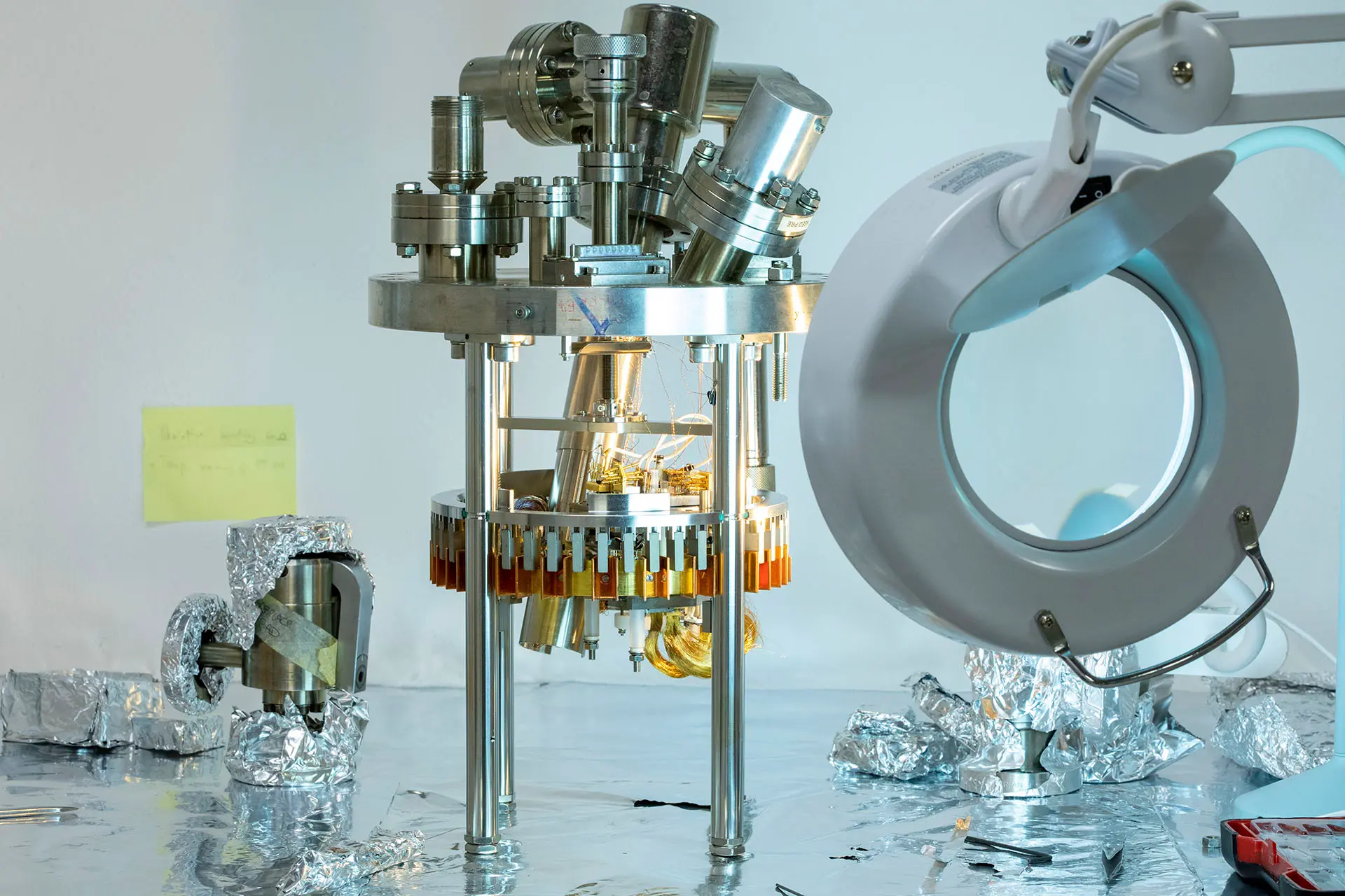
Our experimental apparatus consists of a preparation (MBE) chamber and the STM one which houses a Variable Temperature STM (Omicron Nanotechnology).
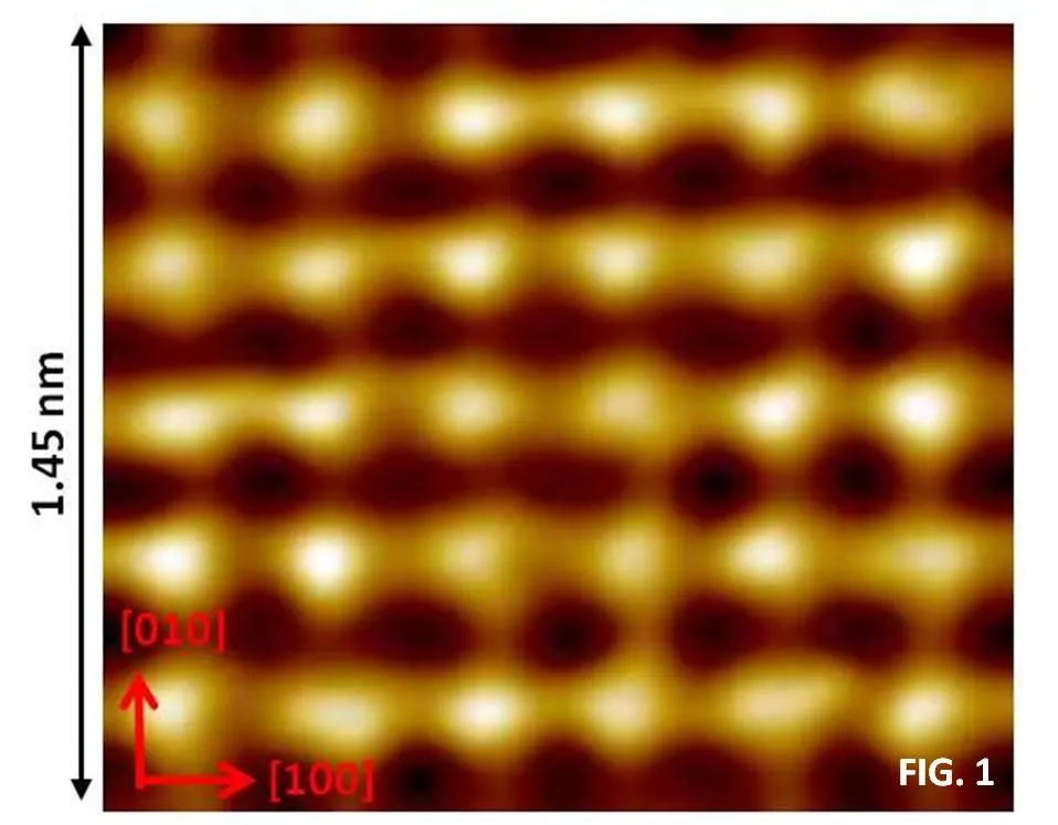
Laboratory activity: our researches are devoted to the deposition and characterization of ultra-thin (few nm) and thin (up to 30 nm) magnetic films (technological applications in data storage and device miniaturization). Among different magnetic substrates, metal overlayers can be grown onto a passivated iron substrate, called Fe(001)-p(1x1) O, that can enhance the magnetic coupling at the metal-metal interface. In Fig.1, we report an atomic resolved image of the Fe(001)-p(1x1)/O substrate.
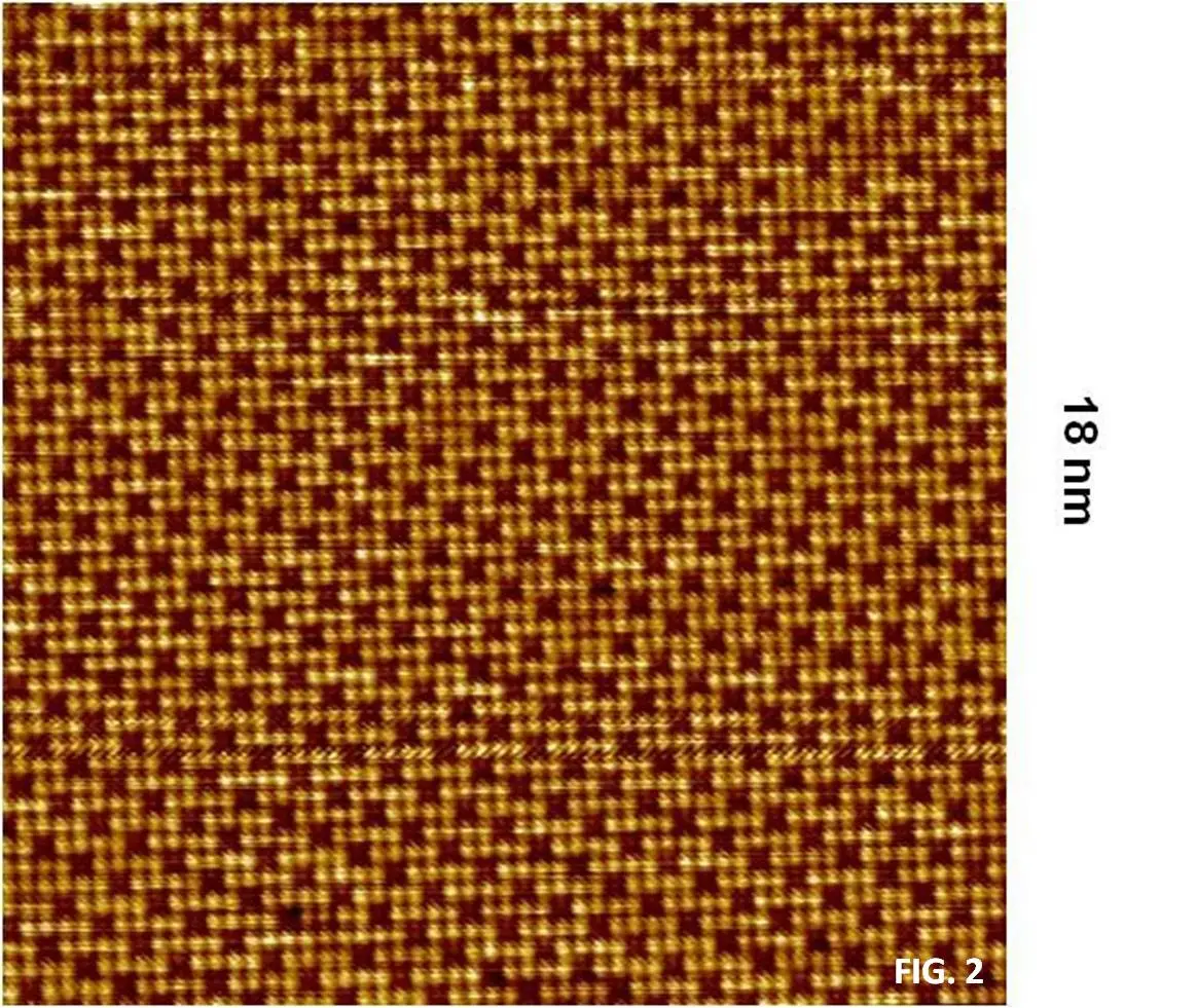
This pre-oxidized iron surface also plays a key role in the growth of metal-oxide systems (namely Ti, Cr, Fe, Co, Ni, Au). In this view, Cr films and Cr-O systems are interesting samples due to their application in devices that show the well known giant magnetoresistance effect. STM microscopy acquires images of the real Cr surface during each step and, consequently, a directly checks the atomic reconstruction of the sample. Fig.2 shows a typical Cr reconstruction, obtained when a single layer of Cr atoms is deposited onto the Fe(001)-p(1x1)/O substrate.

