Study of insulators and semicondutors by means of ultrafast electron microscopy
Study of insulators and semicondutors by means of ultrafast electron microscopy
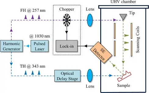
The development of femtosecond electron sources makes it now possible to study ultrafast electron dynamics by a novel technique called Ultrafast Electron Microscopy, which combines the spatial resolution of an Electron Microscope (EM) and the temporal resolution typical of an ultrafast optical pump-probe configuration: the sample is excited by two ultrashort pulses, one optical and one electronic, and the secondary elecrons emissione is measured as a function of the delay between the two pulses. The nanometer escape depth of the SE probe gives the potential to address dynamics at surfaces and interfaces of today's nano-scale devices, where many applications rely on the interplay between semiconductors and insulators.
During the thesis, the student will contribute to the development and the measurements of imaging and spectroscopic tools time resolved, working with ultrafast and nanoscopic capabilities, to be applied mainly to the study of organic and inorganic electronics, as well as insulators (applied by our group for the first time in literature, see Ultramicoscopy 187, 93-97 (2018) Zani et al.) and semiconductors.
The thesis will be developed in collaboration with the Center for Nano Science and Technology (CNST) of the Italian Institute of Technology (IIT).
