USEM
USEM

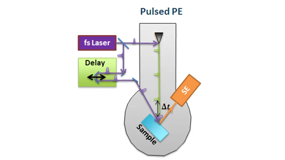
New ultrafast THz electronics based on nanostructures and low-dimensional materials require characterization on extremely small space and time scales. One promising approach is the ultra-fast electron scanning microscopy (USEM). This still pioneering technique has the potential to join the nanoscale spatial resolution of scanning electron microscopy (SEM) with the ultra-fast time resolution of laser photonics to achieve frontier surface-physics characterizations. In short, in a scanning electron microscope (SEM) ultrafast laser pulses on the femtosecond scale excite the sample, whose dynamics is analyzed by electron pulses finely delayed in pump-probe configuration (fig.2).
The Ultrafast Scanning Electron Microscopy (USEM) project raises from the joint effort of Dipartimento di Fisica, CNST-IIT and IFN-CNR, aiming at developing the technique and applying it to the investigation of innovative materials for electronics, sustainable energy harvesting and photonics. EMlab, born in 2013 as a follow-up of the former Scanning Electron Microscopy laboratory, bases its activity on a blend of expertise in electron microscopy, photonics and material science.
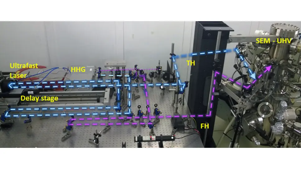
Two experimental setups are under development. One of the first worldwide Ultrafast Scanning Electron Microscope was custom devised based on a ultrahigh vacuum Scanning Auger apparatus endowed with in-situ preparation facilities (ion sputtering, heating up to 1200 °C) and is hosted at Dipartimento di Fisica. It works in pump-probe regime reaching below 10 ps in time resolution. (fig.3)
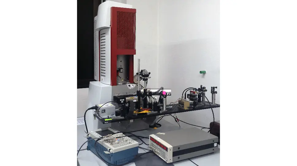
A second apparatus, hosted at CNST-IIT, was adapted from a commercial FEG SEM and is aimed at the highest spatial resolution, either achieving sub-microsecond time resolution in pump-probe mode or working in real-time mode at time scales of second and longer.
The first scientific outcome was obtained in the investigation of color centers at the surface of Alumina films (Zani et al., 2017) for application as gate insulator in electronics, while the current efforts are devoted to the investigation of photoinduced charge dynamics in hybrid perovskite films and at surfaces of inorganic semiconductors, as a function of doping and adatom concentration. (fig.4)
The present activity focuses on the following objectives:
- the investigation of prototypical and frontier materials
- the technical development and optimization of coherent pulsed electron and photon sources for the investigation of photoexcited dynamics in condensed matter by electron microscopy
- the experimental characterization and theoretical understanding of the information accessed by time resolved SEM
BSc and PhD Thesis are available on several threads:
- condensed matter investigation by USEM and complementary techniques
- numerical modeling of electron pulse generation, electron pulse transport in the microscope optics, and electron–matter interaction dynamics
- development of electron and photon sources, and of electron detectors for time-resolved electron microscopy


